Ion Energy BMS Wiring [PDF]
1 Connector and pins configuration 1.1 BMS connectors general descrition 1 5 2 6b 4 8 3 9 6a 7b 7a Figure 1: FS
42 0 2MB
Papiere empfehlen


![Ion Energy BMS Wiring [PDF]](https://vdoc.tips/img/200x200/ion-energy-bms-wiring.jpg)
- Author / Uploaded
- Ilayaraja Boopathy
Datei wird geladen, bitte warten...
Zitiervorschau
1 Connector and pins configuration 1.1
BMS connectors general descrition
1 5 2
6b
4
8
3 9
6a
7b 7a
Figure 1: FS-LT connectors top view N° 1 2 3 4 5 6a 6b 7a & 7b 8 9
Connector Isolated CAN Cells connector Thermistors connector GPIO connector PDU connector Micro SD card SD card extension
Pins 8 26 10 16 10 7
Programming connector
5
External isolated reset Extension & debug
2 15
Table 1: FS-LT connectors Description Isolated CAN bus (1500V) for communication with external devices Connect to battery cell terminals Connect to 10k NTC resistor for temperature sensing Digital, analog isolated and non-isolated I/O. Connect to PDU. Drive the power switch and measure power current Used only to connect an external SD connector Connect to programming tool for loading a new firmware Used to force a BMS reset Reserved
All connectors needed for the BMS implantation in its system (1 to 5) are from the JST PUD family. See here for a complete datasheet of these connectors: http://www.jst-mfg.com/product/pdf/eng/ePUD.pdf All the needed references are described in the table below. Onboard connector N° Manufacturer 1
JST
2
JST
3
JST
4
JST
5
JST
Table 2: Recommended complementary connectors Recommended complementary connector Part number Manufacturer Part number PUDP-08V-S S08B-PUDSS-1 JST SPUD-001T-P0.5 with AWG 24 PUDP-26V-S S26B-PUDSS-1 JST SPUD-001T-P0.5 with AWG 24 PUDP-10V-S S10B-PUDSS-1 JST SPUD-001T-P0.5 with AWG 24 PUDP-16V-S S16B-PUDSS-1 JST SPUD-001T-P0.5 with AWG 24 PUDP-10V-S S10B-PUDSS-1 JST SPUD-001T-P0.5 with AWG 24
3
1.2
Mechanical data
3D files (.step and .pdf) are available here: ZIP archive
L1
L2
Table 3: external dimensions (mm) of FS-LT L1 L2 H H1 H2 H3
H3
E
H
H2 H1
E
110 62 15.95 9.5 8.5 4.85 1.6
K
Figure 2: Mechanical view (top and side) external dimensions of the board
F
M
L
O
J
G
C
D
H
E
I
N
O
Table 4: FS-LT dimensions (mm)
P
B
Figure 3: Mechanical view (top side) connectors and mounting holes positions
A B C D E F G H I J K L M N O P
21.5 20.8 18 13.8 12 3 12 28 10 18 3 3 24.4 9.4 6 Þ4
The mounting holes are designed to receive M3 screw head. Any M3 screw, or other screw with similar specification, can be used. A specification of M3 screw can be found here: http://www.fasnetdirect.com/refguide/MetD7985a.pdf
4
1.3
Cells connector n°2 Table 5: Cell connector part numbers Complementary Crimp reference reference PUDP-26V-S SPUD-001T-P0.5
Connector reference on PCB S26B-PUDSS-1 Figure 4: S26B-PUDSS-1
1
3
5
7
2
4
6
8 10 12 14 16 18 20 22 24 26
Figure 5: PUDP-26V-S
Recommended wire size AWG24 Figure 6: crimp SPUD-001T-P0.5
9 11 13 15 17 19 21 23 25
See Cell configuration p11 and Annexes p15 for more details on the cell connections. The following table shows the cell potentials when every pin is used. Pin n° 1 2 3 4 5 6 7 8 9 10 11 12 13 14 15 16 17 18 19 20 21 22 23 24 25 26
Table 6: Cell connector pins description Type Description Analog input Cell 25+ 1 Analog input Cell 24+ / Cell 25- 1 Analog input Cell 23+ / Cell 24- 1 Analog input Cell 22+ / Cell 23- 1 Analog input Cell 21+ / Cell 22- 1 Analog input Cell 20+ / Cell 21- 1 Analog input Cell 19+ / Cell 20- 1 Analog input Cell 18+ / Cell 19- 1 Analog input Cell 17+ / Cell 18- 1 Analog input Cell 16+ / Cell 17- 1 Analog input Cell 15+ 2 / Cell 16- 1 Analog input Cell 14+ / Cell 15- 2 Analog input Cell 13+ / Cell 14- 2 Analog input Cell 12+ / Cell 13- 2 Analog input Cell 11+ / Cell 12- 2 Analog input Cell 10+ / Cell 11- 2 Analog input Cell 9+ / Cell 10Analog input Cell 8+ / Cell 9Analog input Cell 7+ / Cell 8Analog input Cell 6+ / Cell 7Analog input Cell 5+ / Cell 6Analog input Cell 4+ / Cell 5Analog input Cell 3+ / Cell 4Analog input Cell 2+ / Cell 3Analog input Cell 1+ / Cell 2Analog input Cell 1-
1
In red: pins not used on the 15S and 10S version, only connected on the 25S version
2
In green: pins not used on the 10S version, only connected on the 15S and 25S version
5
1.4
NTC connector n°3 Connector reference on PCB S10B-PUDSS-1 Figure 7: S10B-PUDSS-1
1
3
5
7
2
4
6
8 10
2
Figure 8: PUDP-10V-S
Recommended wire size AWG24 Figure 9: crimp SPUD-001T-P0.5
9
Pin n° 1 2 3 4 5 6 7 8 9 10 1
Table 7: NTC connector part numbers Complementary Crimp reference reference PUDP-10V-S SPUD-001T-P0.5
Table 8: NTC connector pins description Type Description Input NTC5+ 1 Input NTC5- 1 Input NTC4+ 1 Input NTC4- 1 Input NTC3+ 2 Input NTC3- 2 Input NTC2+ Input NTC2Input NTC1+ Input NTC1-
In red: pins not used on the 15S and 10S version, only connected on the 25S version
In green: pins not used on the 10S version, only connected on the 15S and 25S version
6
1.5
PDU connector n°5 Connector reference on PCB S10B-PUDSS-1 Figure 10: S10B-PUDSS-1
1
3
5
7
2
4
6
8 10
Table 9: PDU connector part numbers Complementary Crimp reference reference PUDP-10V-S SPUD-001T-P0.5 Figure 11: PUDP-10V-S
Recommended wire size AWG24 Figure 12: crimp SPUD-001T-P0.5
9
Pin n° 1 2 3 4 5 6 7 8 9 10
Table 10: PDU connector pins description Type Description Digital input Short circuit clear NC Not connected Digital input Precharge circuit command Digital output Short circuit detection Digital input Charge circuit command Analog input Current measurement Digital input Discharge circuit command Analog input PDU Board temperature Supply GND BMS Supply 3.3V BMS
7
1.6
Isolated CAN connector n°1 Connector reference on PCB S08B-PUDSS-1 Figure 13: S08B-PUDSS-1
1
3
5
7
2
4
6
8
Pin n° 1 2 3 4 5 to 8
Table 11: Isolated CAN connector part numbers Complementary Crimp reference Recommended wire reference size PUDP-08V-S SPUD-001T-P0.5 AWG24 Figure 14: PUDP-08V-S
Figure 15: crimp SPUD-001T-P0.5
Table 12: Isolated CAN connector pins description Type Description Supply GND CAN CAN CAN L CAN CAN H Supply 5V CAN NC Not connected
8
1.7
GPIO connector n°4 Table 13: GPIO connector part numbers Complementary Crimp reference reference PUDP-16V-S SPUD-001T-P0.5
Connector reference on PCB S16B-PUDSS-1 Figure 16: S16B-PUDSS-1
1
3
5
7
2
4
6
8 10 12 14 16
Figure 17: PUDP-16V-S
Recommended wire size AWG24 Figure 18: crimp SPUD-001T-P0.5
9 11 13 15
Pin n° 1 2 3 4 5 6 7 8 9 10 11 12 13 14 15 16
Table 14: GPIO connector pins description Type Description Supply 3.3V BMS Supply GND BMS Digital output Open drain n°0 Digital output Open drain n°1 Insulated digital OUT0+ output OUT0Insulated digital IN0+ input IN0Digital I/O GPIO2 Digital I/O GPIO4 Digital I/O GPIO1 Digital I/O GPIO3 Supply GND BMS CAN CAN L CAN CAN H Supply 5V BMS
9
1.8
SD card extension connector n°6a
Connector reference on PCB: B7B-ZR Complementary connector reference: ZRH-7 Crimp contact reference: SZH-002T-P0.5
1 2 3 4 5 6
Pin n° 1 2 3 4 5 6 7
7
Type Description Supply GND BMS Supply 3.3V BMS SPI SDI SPI SCK SPI SDO SPI CS Digital input Card Detect Table 15: SD extension connector pins description
Figure 19: SD extension connector front view
1.9
Programming connector n°7a & 7b
7a directly printed on the PCB (reference: AVX 009159010061916) 7b is a standard 2.54mm pitch connector in parallel of Prog1.
1.10 External isolated reset connector n°8 2.54mm pitch connector. It is an insulated input used to reset the microcontroller. It must be driven with a voltage between 3.3V and 12V.
1
2
Figure 20: External isolated reset connector front view
Pin n° Type Description 1 Insulated digital ResetISO+ input 2 ResetISOTable 16: External isolated reset connector pins description
1.11 Extension - connector 9 Reserved for future uses.
1.12 Harnesses specifications Every standard harness specification can be found in this document: DFM - Harness sets
10
2 General recommendations 2.1
Cell configuration
Every cell harness configurations are presented in annex. See Annexes p15 for more details. If the maximum number of cells are not connected to the BMS, all the unused pins of the cell connector must be shunted. For shunting the unused inputs, there are 2 two solutions: -
Depending on the BMS board version, there can be switches mounted on the PCB for shunting the unused cells. See next figure showing the switches on the PCB. The shunt can be made by connecting the unused input to the previous cell potential.
SW1 is on top
SW2 is on bottom, only mounted for 25S version
Figure 21: Switches for shunting unused cell inputs
2.1.1
Example for a 13S Battery
The battery used for this example has 13 cells in series. The BMS used in this example is a 15S version with shunting switches. Table 17: Cell connector and shunting switches configuration for 13S battery Cell connector Pin n° 1 2 3 4 5 6 7 8 9 10 11 12 13
Description NC NC NC NC NC NC NC NC NC NC Cell 13+ NC Cell 12+ / Cell 13-
Pin n° 14 15 16 17 18 19 20 21 22 23 24 25 26
SW1 switch Description Cell 11+ / Cell 12Cell 10+ / Cell 11Cell 9+ / Cell 10NC Cell 8+ / Cell 9Cell 7+ / Cell 8Cell 6+ / Cell 7Cell 5+ / Cell 6Cell 4+ / Cell 5Cell 3+ / Cell 4Cell 2+ / Cell 3Cell 1+ / Cell 2Cell 1-
11
switch n° 1 2 3 4 5 6
Switch state ON OFF ON OFF OFF OFF
See FS-LT AN 48V documents for more details
14
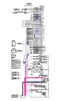
Figure 22: example of FS-LT-15S + FSB-PR-I implementation diagram
3 Short example with 15S battery and contactors
4.3.2
20S battery with 25S BMS board Table 54: 20S battery cell harness with 25S BMS board (with shunting switches) Cell connector
Pin n° 1 2 3 4 5 6 7 8 9 10 11 12 13
Description Cell 20+ NC Cell 19+ / Cell 20Cell 18+ / Cell 19Cell 17+ / Cell 18Cell 16+ / Cell 17NC Cell 15+ / Cell 16Cell 14+ / Cell 15Cell 13+ / Cell 14Cell 12+ / Cell 13NC Cell 11+ / Cell 12-
SW1 switches
Pin n° 14 15 16 17 18 19 20 21 22 23 24 25 26
Description Cell 10+ / Cell 11Cell 9+ / Cell 10Cell 8+ / Cell 9NC Cell 7+ / Cell 8Cell 6+ / Cell 7Cell 5+ / Cell 6Cell 4+ / Cell 5NC Cell 3+ / Cell 4Cell 2+ / Cell 3Cell 1+ / Cell 2Cell 1-
Switch n° 1 2 3 4 5 6
Switch state ON OFF ON OFF ON OFF
SW2 switches Switch n° 1 2 3 4
Switch state ON OFF ON OFF
Table 55: 20S battery cell connector pins description with 25S BMS board (NO shunting switches) Cell connector Pin n° 1 2 3 4 5 6 7 8 9 10 11 12 13
Description Cell 20+ Cell 19+ / Cell 20Cell 19+ / Cell 20Cell 18+ / Cell 19Cell 17+ / Cell 18Cell 16+ / Cell 17Cell 15+ / Cell 16Cell 15+ / Cell 16Cell 14+ / Cell 15Cell 13+ / Cell 14Cell 12+ / Cell 13Cell 11+ / Cell 12Cell 11+ / Cell 12-
Pin n° 14 15 16 17 18 19 20 21 22 23 24 25 26
32
Description Cell 10+ / Cell 11Cell 9+ / Cell 10Cell 8+ / Cell 9Cell 7+ / Cell 8Cell 7+ / Cell 8Cell 6+ / Cell 7Cell 5+ / Cell 6Cell 4+ / Cell 5Cell 3+ / Cell 4Cell 3+ / Cell 4Cell 2+ / Cell 3Cell 1+ / Cell 2Cell 1-